
Basic knowledge of MOS tube
MOS tubes can be divided into enhancement type and depletion type, enhancement type is divided into P channel and N channel, and depletion type is also divided into P channel and N channel. In practical applications, what we call NMOS and PMOS are both Refers to N-channel and P-channel enhancement MOS transistors. So the MOS tubes we are talking about here are both types. For these two MOS tubes, we usually use NMOS for the following reasons:
1. The on-resistance is small, and the resistance of several milliohms can be achieved, and the conduction loss is small.
2. The input resistance is very high, can reach hundreds of millions of ohms, almost no current.
3. Fast switching speed and low switching loss, especially suitable for switching power supply.
4. Strong current handling capability.
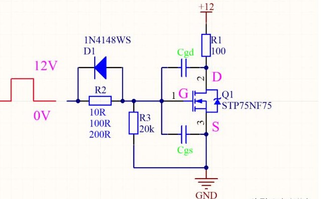
There is a parasitic capacitance between the three pins of the MOS tube. This cannot be changed by us. It is caused by the manufacturing process, so there will be some factors that we must consider when designing the circuit.
Switching characteristics of MOS tube
1. P-channel MOS tube switch circuit
The characteristics of PMOS, Vgs is less than a certain value will be turned on, suitable for the situation when the source is connected to VCC (high-side drive). It should be noted that Vgs refers to the voltage of the gate G and the source S, that is, the gate is turned on when it is lower than a certain voltage of the power supply, not the voltage relative to the ground. However, because the PMOS conduction internal resistance is relatively large, it is only suitable for low power situations. High power still uses N-channel MOS transistors.

2. N-channel MOS tube switch circuit
The characteristics of NMOS, when Vgs is greater than a certain value, it will be turned on. It is suitable for the situation when the source is grounded (low-side drive). As long as the gate voltage is greater than the Vgs given in the parameter manual, the drain D is connected to the power supply. , the source S is grounded. It should be noted that Vgs refers to the voltage difference between the gate G and the source S, so when the NMOS is used as a high-side driver, when the drain D and the source S are turned on, the potential of the drain D and the source S are equal, then The gate G must be higher than the voltage of the source S and the drain D, so that the drain D and the source S can continue to conduct.
MOS tube switch circuit example 1 (MOS tube is used to control the load)
Conduction condition: Vgs>Vth, the function of R1 and R2 is to create a Vgs voltage between G and S, and there is no need to care about the voltage relationship between G and D (as long as the breakdown voltage is not reached). In addition, the S pole does not necessarily need to be grounded, as long as the potential difference between Vg and Vs is greater than Vth, the MOS tube can still function as a switch.
Things to note:
1. The maximum driving peak current of the IO port, the driving capability of the IO port of different chips is different.
2. Understand the parasitic capacitance of the MOS tube. If the parasitic capacitance is large, the energy required for conduction is greater. If the peak value of the output current of the IO port is small, the conduction of the tube will be slower.
MOS tube switch circuit example 2 (MOS tube control power output)
Here we use NPN and NMOS transistors for switch design as shown in Figure 4. When Q2 inputs a low level, the triode Q2 does not conduct, the Vgs of the MOS transistor Q1=0, and the MOS transistor Q1 does not conduct. When the input level of Q2 is high, the triode is turned on, the Vgs and Vth of the MOS transistor Q1 are turned on, and the MOS transistor Q1 is turned on. Due to the conduction of the MOS tube
Matters needing attention:
1. Pay attention to the direction of the diode between the MOS tubes D and S. When it is not conducting, the direction of the diode should be opposite to the direction of the power output.
2. Since there is internal resistance when the MOS tube is turned on, the output voltage of the MOS tube is lower than the actual input voltage.
Ebyte is a national high-tech enterprise specializing in the research and development of wireless modules and industrial IoT terminals. Independently developed and produced products include LoRa/WiFi Wireless Module/Bluetooth/ZigBee wireless modules, 4G networking equipment, Ethernet modules, NB-IoT data transmission terminals, and industrial IoT.


