
Common Mode Interference is a common type of interference in electronic circuits and communication systems. It corresponds to another type of interference called Differential Mode Interference.
In electronic circuits, signals can be transmitted in two modes: differential mode and common mode.
ARTICLE OUTLINE
Overview of Differential Mode Interference 1. Common mode 3. Methods to Solve Differential Mode Interference |
This mode involves two signal lines simultaneously affected by the same external interference. This interference can come from power lines, electromagnetic fields, RF interference, and more. As the interference on both signal lines is the same, the common mode gain in the circuit amplifies this interference, leading to a degradation of system performance.

This mode involves two signal lines transmitting positive and negative signals, and the difference between the signals is amplified to extract the useful data. Differential mode transmission has good immunity to interference because it cancels out the effects of external interference on the two signal lines.
Methods to Solve Differential Mode Interference
1. Using differential signaling: Implementing insulation amplifiers or isolation transformers in the design to separate the differential signals and avoid the impact of common mode signals on grounding.
2. Reducing common mode noise: Designing suitable filters, using low-noise power supplies, and other methods to reduce the level of common mode noise and minimize common mode interference.
3. Optimizing grounding circuits: In PCB design, plan the grounding layout carefully, reduce grounding paths, lower ground resistance, and avoid creating loops that could have adverse effects.
4. Adding protective measures: Employ shielding techniques, shielded cables, etc., to protect against external electromagnetic fields and reduce differential mode interfere
5. Improving signal integrity: Utilize appropriate signal control techniques, such as differential driving and differential receiving, to enhance signal integrity and immunity to interference.
In summary, eliminating common mode interference requires a comprehensive consideration of factors such as signal sources, receivers, transmission media, and grounding. Corresponding optimization and improvement measures should be taken. In high-speed PCB designs, differential signaling is increasingly used due to its advantages in strong immunity to interference, effective EMI suppression, and precise timing positioning.
China Wireless modem Manufacturer,Industrial IoT terminals ExpertModem & DTU sale .Chengdu Ebyte Electronic Technology Co., Ltd is a well-known China Wireless modem Manufacturer and Industrial IoT terminals Expert, focusing on IOT communication applications. Modem & DTU cover CAN bus, data transmission radio stations, industrial routers/gateways, LORAWAN, remote I/O modules, Industrial signal transmission, etc., with nearly 100 inventions and utility model patents, and the products have passed SRRC, FCC, CE, MIC, KC, NCC, and other authoritative certifications. Get in touch with ONLINE SERVICE to discover how our projects work for you! |
Application Wiring Requirements
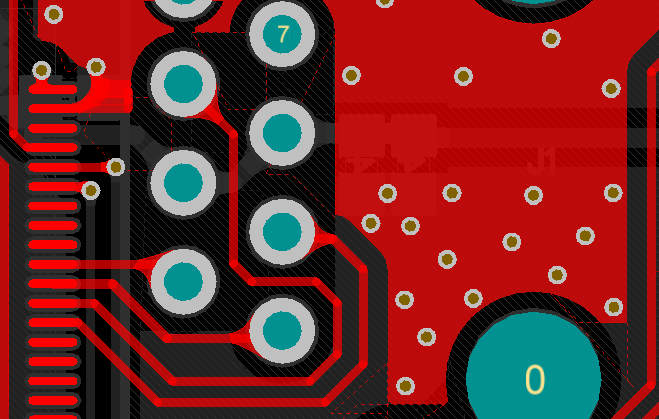
On the circuit board, differential traces must be two lines of equal length, equal width, close proximity, and on the same level.
▶ Isometric: Equal length means that the length of the two lines should be as long as possible, in order to ensure that the two differential signals keep opposite polarities at all times. reduce common mode components.
▶ Monospaced, equidistant: Equal width means that the trace widths of the two signals need to be consistent, and equidistant means that the distance between the two lines should remain unchanged and parallel.
▶ Minimum change in impedance: When designing a PCB with differential signals, one of the most important things is to determine the target impedance for the application and plan the differential pairs accordingly. Furthermore, impedance changes are kept as low as possible. Differential line impedance depends on factors such as line width, line coupling, copper thickness, PCB material, and stack up
Consider the above when you are trying to avoid anything that changes the differential impedance.

Misunderstanding
1: It is believed that differential signals do not require a ground
plane as a return path, or that differential traces provide each other
with a return path. The reason for this misunderstanding is the
confusion of superficial phenomena or insufficient understanding of the
mechanism of high-speed signal transmission. Differential circuits are
insensitive to similar and other noise signals that may be present on
the power supply and ground. In PCB circuit design, the coupling between
differential lines is usually low, usually 10% to 20% of the coupling
degree, and more is coupled to the ground, so the main return path of
differential traces always exists on the ground plane. When a local
plane is broken without a reference plane, the coupling between the
differential traces will provide the main loop, although the impact of
the reference plane break on the differential traces is not serious for
single-ended traces, it reduces the differential signal quality, and
potentially increases EMI, so try to avoid it.
Misunderstanding 2: Thinking that maintaining equal spacing is more important than matching line lengths. In actual PCB layout, the requirements of differential design often cannot be met at the same time. Due to factors such as pin distribution, via holes and line space, the goal of line length matching must be achieved through appropriate winding, but the result is: the differential line One part cannot be parallel. The most important rule in the design of PCB differential routing is to match the line length, and other rules can be handled flexibly according to design requirements and practical applications.

Misunderstanding
3: It is believed that the differential traces must be close together.
The proximity of differential lines is nothing more than strengthening
their coupling, improving immunity to noise, and making full use of the
opposite polarity of the magnetic field to offset external
electromagnetic field interference. While this method is very useful in
most cases, it is not absolute, if we ensure that they are completely
free from external interference, we will no longer need to allow strong
communication between each other to achieve the goal of preventing
interference and suppressing EMI.
How
to ensure good isolation and protection of differential lines? Increasing the distance from other signal lines is one of the most basic
methods. The electromagnetic field energy decreases according to the
square relationship of the distance. When the total distance between
lines is 4 times the line width, the interference between them is very
weak, and basically ignored.
In addition, the isolation through the ground plane can also play a good shielding role. This structure is often used in high-frequency (above 10G) IC package PCB design. It is called CPW structure, which can ensure strict differential impedance. control. In addition, ground plane insulation can also play a good shielding role. This structure is often used in high-frequency (above 10g) IC shell PCB structures, called CPW structures, which can achieve strict differential impedance control.


