


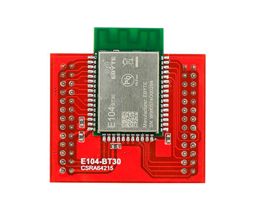
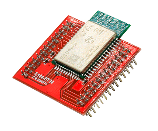
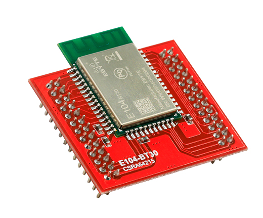
[Interface]:PCB
[Chip]:CSRA64215
[Introduction]:E104-BT30-TB1 is a multifunctional and cost-effective module developed by our company for audio Bluetooth transmission. The main control uses the CSRA64215 chip of CSR to provide the module with high-quality sound and compatibility. The Bluetooth module uses a driver-free method. Users only need to connect the module to the application product to quickly achieve high-quality Bluetooth audio transmission and enjoy wireless music. And the module supports APTX, APTXLL, ACC and other high-quality sound effects.
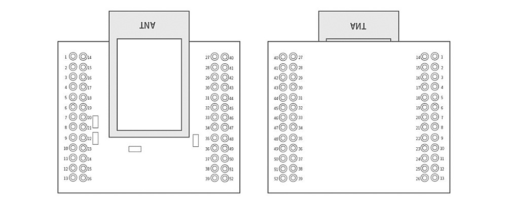
| Pin No. | Pin item | Pin direction | Application |
| 1 | GND | P | Ground, connect to power reference ground |
| 2 | PIO4 | I/O | SPI-CS debug load pin |
| 3 | PIO3 | I/O | SPI-MISO debug load pin |
| 4 | PIO17 | I/O | AUX input trigger pin(reserved function) |
| 5 | PIO3 | I/O | SPI-MISO debug load pin |
| 6 | Reserve | O | Unused |
| 7 | Reserve | O | Unused |
| 8 | VREGENABLE | I | Bluetooth module power-on / power-off control pin, high level is effective. |
| 9 | GND | P | Ground, connect to power reference ground |
| 10 | Reserve | O | Unused |
| 11 | PIO18 | I/O | General-purpose I / O (reserved function) |
| 12 | VBAT_SE | P | Battery charge sensing input (reserved function) |
| 13 | GND | P | Ground, connect to power reference ground |
| 14 | VBAT-IN | P | Battery power input pin, cannot exceed 3.6V, otherwise the module will be damaged |
| 15 | CHG_EXT | P | External battery charger control (reserved function) |
| 16 | USB-DP | I/O | USB cable positive (reserved function) |
| 17 | USB-DP | I/O | USB cable negative (reserved function) |
| 18 | VCHG | P | Internal charger input, usually connected to VBUS, see Typical application circuit for details |
| 19 | RST | I | Module reset pin, pull down for 5ms to trigger reset |
| 20 | SPI-PCM | I | SPI/PCM input selection, 0=PCM/PIO interface, 1=SPI |
| 21 | LED2 | O | Bluetooth status indication LED2 driver output |
| 22 | LED0 | O | Bluetooth status indication LED0 driver output |
| 23 | PIO5 | I/O | SPI-CLK debug load pin |
| 24 | PIO2 | I/O | SPI-CLK debug load pin |
| 25 | PIO16 | I/O | Module audio output indication pin, high level is effective |
| 26 | AIO0 | I/O | Analog programmable I/O pin 0 (reserved function) |
| 27 | GND | P | Ground, connect to power reference ground |
| 28 | Reserve | O | Unused |
| 29 | Reserve | O | Unused |
| 30 | Reserve | O | Unused |
| 31 | Reserve | O | Unused |
| 32 | Reserve | O | Unused |
| 33 | PIO9 | I/O | Play / Pause Key input, high level effective |
| 34 | PIO7 | I/O | Volume + Key input, high level effective, long press to continuously |
| 35 | VDD-PADS-2 | P | Input and output port power 2, usually 1.8V power connection |
| 36 | 1V8-SMPS | P | Module 1.8V power output, external decoupling capacitor is recommended, see 4.2 Recommended circuit for details |
| 37 | VDD-PADS-1 | P | Input and output port power supply 1, usually 1.8V power supply connection |
| 38 | PIO8 | I/O | Previous song Key input, high level is effective |
| 39 | PIO6 | I/O | General-purpose I / O (reserved function) |
| 40 | GND | P | Ground, connect to power reference ground |
| 41 | MIC-AN | I | Channel A line or microphone input negative |
| 42 | MIC-AP | I | Channel A line or microphone input positive |
| 43 | LINE-BN | I | Channel B line input negative |
| 44 | LINE-BP | I | Channel B line input positive |
| 45 | MIC-BIAS | I | Microphone bias |
| 46 | PIO0 | I/O | Volume - Key input, high level effective, long press to continuously |
| 47 | SPK-LN | O | Left channel speaker output negative |
| 48 | SPK-LP | O | Left channel speaker output positive |
| 49 | SPK-RP | O | Right channel speaker output positive |
| 50 | SPK-LN | O | Left channel speaker output negative |
| 51 | PIO1 | I/O | Next song Key input, high level is effective |
| 52 | PIO21 | I/O | General-purpose I / O (reserved function) |