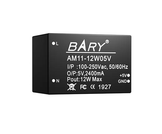

The rectification method at the external interface is as follows:
1. The rectification method for the USB interface: add an ESD chip (such as SRV05-4) to the USB signal line D+, D-, and add a TVS diode protection on the power line to prevent interference.
Some suggestions on PCB layout:
2. For the rectification of the power supply layout: as shown in Figure 1,
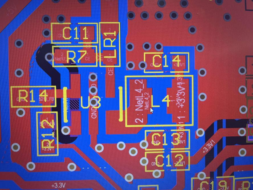
The layout of the DCDC power supply passes through the inductor at the voltage output end. The layout of the bypass capacitor and the energy storage capacitor is shown in the figure. The bypass capacitors C14 and C13 are as close as possible to the inductor output. It is best to take the voltage after passing through the capacitor C12. The purpose is that the circuit can filter better and reduce interference.
Related article:
3. All the high-frequency bypass capacitors passing through the power line and signal line should be grounded as close as possible to reduce the large ESD current entering the circuit system and play a better role in absorbing interference.
4. Reset line, restore the factory signal line, as short as possible, because the longer the line, the harder it is to withstand the ESD energy, so the layout of the components should be as close as possible to shorten the length of the line: if it is unavoidable, the line The two sides of the chip should be wrapped as much as possible, as shown in Figure 2: the purpose is to reduce other signal interference, avoid interference, and restart the chip without reason. At the same time, capacitors and resistors can be added to the circuit to increase the internal resistance and prevent excessive interference signals.
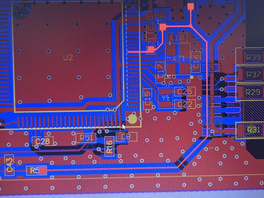
The layout of the switch reset line is also based on the same principle. A π-type filter circuit can be added to the circuit, as shown in Figure 3 below, which can better eliminate external interference and prevent chip reset.

5. To supply power to the chip, the power supply line should pass through the capacitor as much as possible first, and then flow to the chip to protect the chip. As shown in Figure 4

6. Lay copper on the ground wire, try to avoid right angles, which will lead to inconsistent discharge paths, try to use corners greater than 90°, and the sharp corners of the right angle will cause dryness, as shown in Figure 5.
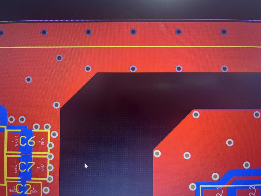
7. The communication line first passes through the protection device, then discharges through the anti-detonator, the anti-detonator is grounded nearby, and then discharges through TVS. The line should be as short as possible and the loop as small as possible, which can quickly eliminate interference signals. Adding a Y capacitor on the ground can quickly discharge and eliminate static electricity.
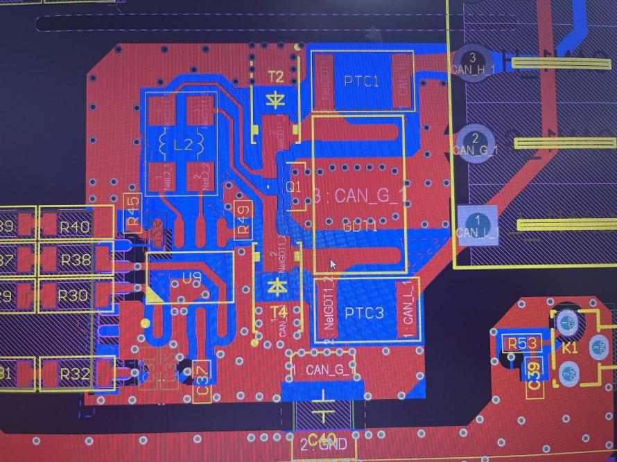
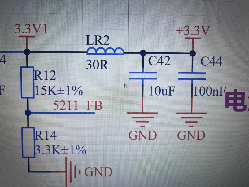
8. MUC and other chips can be powered separately to avoid mutual interference, and an LC filter circuit can be added to the circuit. The circuit is shown in the figure:
9. Multilayer boards can also be used, which can greatly improve the system's ability to resist ESD discharges. Placing the first layer ground plane as close as possible to the signal trace layer allows ESD transients to quickly cancel out when they reach the trace.
10. Plus isolation, electrical isolation is also a method to suppress the impact of electrostatic discharge. Adding isolation chips or optocouplers, transformers, etc. on the PCB, and combining cut-off isolation and shielding can well suppress the impact of electrostatic discharge.
In general, regarding the design of preventing ESD electrostatic interference, the layout of power planes, ground planes and signal lines is one of the important measures for PCB ESD protection design.
Ebyte is a national high-tech enterprise specializing in the research and development of wireless modules and industrial IoT terminals. Independently developed and produced products include LoRa/WiFi Wireless Module/Bluetooth/ZigBee wireless modules, 4G networking equipment, Ethernet modules, NB-IoT data transmission terminals, industrial IoT.


