
The English full name of SPI is Serial Peripheral Interface, as the name implies, it is a serial peripheral interface. SPI is a synchronous serial communication interface specification, mainly used in short-distance communication in embedded systems. The interface was developed by Motorola in the mid-1980s and has since grown into an industry standard.
Article Outline :
SPI is a high-speed, full-duplex, synchronous communication bus, and only needs to use 4 wires at most, which saves the pins of the chip. SPI is mainly used in EEPROM, FLASH, ADC, DAC and other chips, as well as digital Between the signal processor and the digital signal decoder.
SPI devices communicate in full-duplex mode, which is a master-slave mode between a master and one or more slaves. The host is responsible for initializing the frame. This data transmission frame can be used for both read and write operations. The chip select line can select one from multiple slaves to respond to the request of the host.
The SPI interface is defined as follows:

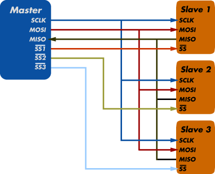
It can also be seen from the above figure that when communicating between SPI devices, the data line should be MOSI connected to MOSI, MISO connected to MISO, and SCLK connected to SCLK instead of reverse connection of TX and RX like serial ports. When there is only a single SPI slave device, if the slave device allows it, the CS/SS line can be fixed at low level directly. However, for chips like MAX1242 that need to be triggered by the falling edge of the CS/SS line, the CC/SS line must be connected to the host. As shown in the figure below, it is a master-slave connection mode.

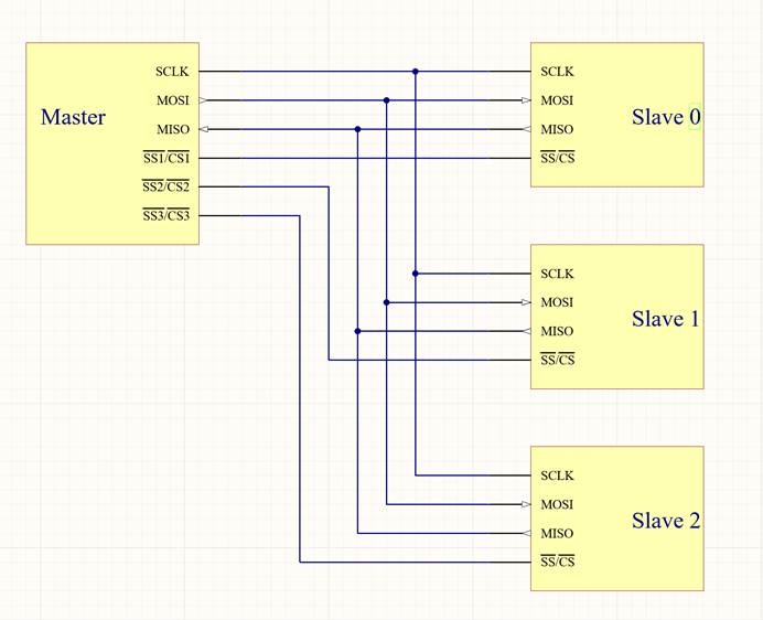
For multiple slave devices, each slave needs a CS/SS line to connect to the host, so that the host can communicate with any slave. The following figure shows the connection mode of one master and multiple slaves.

Most slave devices feature tri-state logic so that their MISO signal line goes to a high-impedance state (electrically disconnected) when the device is not selected. Devices without tri-state output need an external tri-state buffer to share the SPI bus with other slave devices.
In SPI communication, the SPI master device sends the SPI slave device to the SPI slave device through the SCLK line at the frequency supported by the slave device. This also means that the slave device cannot actively send data to the master device. Or the slave device actively informs the host of data arrival through an IO port.
In each clock cycle of SPI, a full-duplex data transmission will be performed. When the host sends 1 bit through the MOSI line, the slave will also send 1 bit data out through the MISO line after reading it. This means that even if only simplex communication takes place, this communication sequence is maintained.
RELATED ARTICLE:
 SPI transfers usually involve two shift registers with a given word size. For example, the 8-bit shift register in the master and slave. They are connected in a virtual ring topology, with data usually being shifted out most significant bit first. On the clock edge, both the master and the slave shift out 1-bit data and give it to each other on the transmission line. When the next clock edge comes, the receivers of both parties sample the bit on the transmission line and set it as the new least significant bit of the shift register. After register bits are shifted out and in, the master and slave exchange register values. If more data needs to be swapped, the shift register is reloaded and the process repeated. A transfer can last for any number of clock cycles. When done, the host stops toggling the clock signal. As shown in the figure below, it is a schematic diagram of the shift register for the interaction between the master and the slave.

The communication flow is as follows:
1. The SPI master first pulls the SS or CS line low to inform the SPI slave that communication starts.
2. The host sends the SCLK clock signal to inform the slave of the upcoming read and write operations. The SCLK clock signal here is determined by the SPI mode whether it is active at high level or at low level, which will be introduced later.
3. The host (Master) writes the data to be sent to the sending data buffer area (Memory), the buffer area passes through the shift register (0~7), and the serial shift register shifts the byte bit by bit through the MOSI signal line. Send out to the slave, and at the same time, the data received by the MISO interface is moved to the receiving buffer one by one through the shift register.
4. The slave (Slave) also returns the contents of its serial shift register (0~7) to the host through the MISO signal line. At the same time, the data sent by the host is received through the MOSI signal line, so that the contents of the two shift registers are exchanged.
4 working modes of SPI communication
There are 4 different operating modes in SPI communication, and different slave devices may be set to a certain mode at the factory and cannot be changed. But SPI communication must be in the same mode to proceed. Therefore, we should configure the mode of the SPI master device in our own hands, that is, control the communication mode of the SPI master device through CPOL (clock polarity) and CPHA (clock phase), as follows:
The clock polarity (CPOL) defines the level at which the SCLK clock line is idle:
1. CPOL=0, that is, SCLK=0, means that the level of the SCLK clock signal line is low in the idle state, so the active state is high.
2. CPOL=1, that is, SCLK=1, which means that the level of the SCLK clock signal line is high in the idle state, so the active state is low.
The clock phase (CPHA) defines the timing (ie phase) of the data bits relative to the clock line:
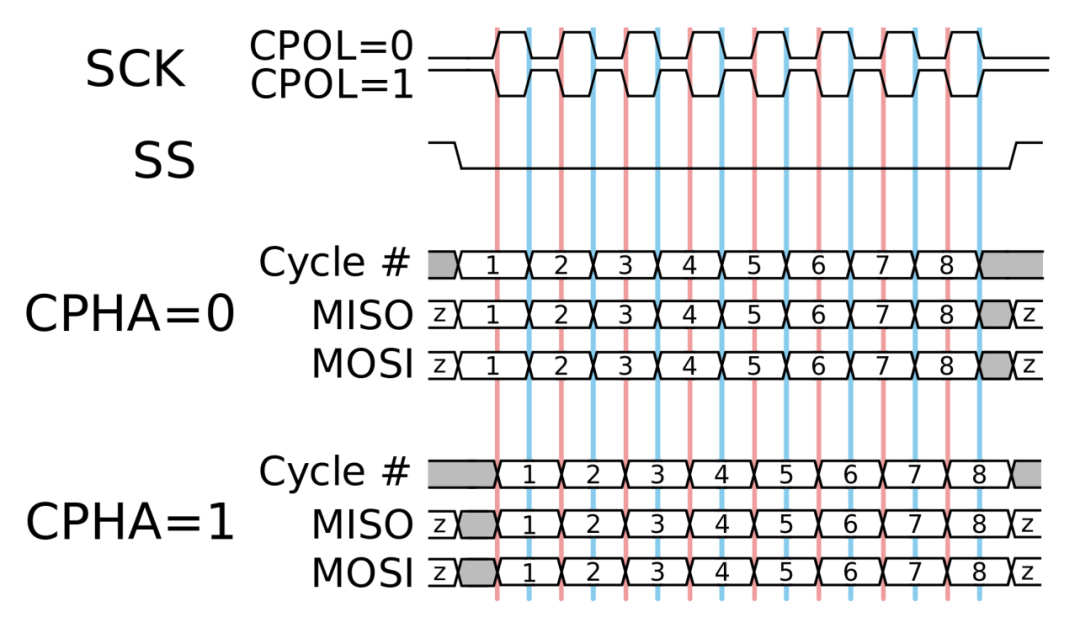
1. CPHA=0, which means that the output (out) terminal changes data on the trailing edge of the previous clock cycle, and the input (in) terminal captures data on the leading edge of the clock cycle (or shortly thereafter). The output remains valid until the trailing edge of the current clock cycle. For the first clock cycle, the first bit of data must appear on the MOSI line before the leading edge of the clock. That is, a CPHA=0 cycle includes half a clock idle and half a clock set cycle.
2. CPHA=1, which means that the output (out) terminal changes data on the leading edge of the current clock cycle, and the input (in) terminal captures data on the trailing edge (or shortly after) of the clock cycle. The output remains valid until the leading edge of the next clock cycle. For the last clock cycle, the slave device holds the MISO line active until the Chip Select signal goes off. That is, a CHPA=1 cycle includes half a clock set and half a clock idle cycle.
Note: The leading and trailing edges here mean the first edge and the last edge in each cycle. Generally speaking: when the clock is a positive clock, the rising edge of the clock line is the leading edge, and the falling edge of the clock is the trailing edge, and vice versa.
The figure below shows the timing diagram for clock polarity and phase. The red line represents the leading edge of the clock, and the blue line represents the trailing edge of the clock.

The advantage of SPI is that it has higher throughput than I2C, is not limited by the maximum clock speed, can realize potential high-speed, extremely simple hardware interface, and the pull-up resistors used by peripheral circuits are less than I2C protocol. It means that it has lower power consumption than I2C, the clock source of the slave comes from the host device, no need to add a precision oscillator, the slave does not need a unique address, and the number of pins used is greatly reduced compared to the parallel interface Etc.
But at the same time, there are certain shortcomings, such as SPI does not have in-band addressing, when using multiple slave devices of different modes, the master device will re-initialize when switching modes, which will slow down the access to the slave device, and the SPI slave device does not have Hardware flow control can only delay the arrival of the next clock cycle independently through the host, and can only communicate in short distances. But if SPI can be applied in the direction of avoiding the shortcomings of SPI, the advantages of SPI make it far superior to other protocols.


